Home » Component data » Transistor data » this page
2N3553 Transistor Data
Key transistor data for the 2N3553 RF power transistor including key electrical parameters, pinout, package type and many other key transistor datasheet details.
The 2N3553 is an epitaxial silicon NPN transistor of the 'overlay' emitter electrode construction type. It is intended for use in class A, B, and C amplifiers, frequency multipliers and oscillators.
As a high power class C amplifier, a circuit using a 2N3553 would typically provide up to 2.5 watts output up to frequencies of 250 MHz or more. Asa high power oscillator it could typically provide 1.5 watts of RF power.
Key details and performance parameters for the 2N3553 transistor.
| Transistor parameters & data |
|
|---|---|
| Parameters | Details |
| Transistor type | NPN silicon RF power transistor |
| Package type | TO39 |
| VCBO max (V) | 65 |
| VCEO max (V) | 40 |
| VEBOmax (V) | 4 |
| IC max (mA) | 1000 peak, 330 continuous |
| TJ Max °C | 200 |
| PTOT W | 7 |
| fT min (MHz) | 500 |
| COB | 35pF max @ 40 MHz 50mA (see datasheet for full curves) |
| hfe | |
| IC for hfe | |
| Similar / equivalents | |
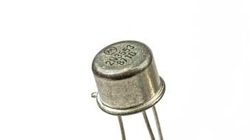
Outline:
![]()
Pinout:
![]()
Explanation of transistor parameters
| Parameter | Explanation |
|---|---|
| VCBO Max | Maximum collector-base voltage with emitter open circuit . |
| VCEO Max | Maximum collector-emitter voltage with base open circuit. |
| VEBO Max | Maximum emitter-base voltage with collector open circuit. |
| VCEsat (included where applicable) | The voltage drop across the collector-emitter when the transistor is fully saturated (acting as a closed switch). |
| IC Max | Maximum collector current. |
| Parameter | Explanation |
|---|---|
| TJ | Maximum junction temperature. |
| PTOT Max | Maximum device dissipation normally in free air at 25°C unless other conditions indicated. |
| fT Min | Minimum cutoff frequency at which the current gain in a common emitter circuit falls to unity. |
| COB Max | Maximum collector capacitane, normally measured with emitter open circuit. |
| hFE | DC current gain for HFE at IC. [Note hfe is the small signal gain and although this may be slightly different, the transistor current gain will vary considerably from ne transistor to the next of the same type.] |
| PTOT Max | Maximum device dissipation normally in free air at 25°C unless other conditions indicated. |
These are the main transistor parameters that have been included in our list. There are others, but these help quantify the main elements of the performance of the transistor.
Please note, that the data given is the best estimate we can give within a tabulated summary of this nature. Parameters also vary between manufacturers. Electronics Notes cannot accept any responsibility for errors, inaccuracies, etc, although we do endevaour to ensure the data is as accurate as possible.
Notes and supplementary information
The 2N3553 was a popular RF power transistor used for a variety of RF driver and output circuits.
• Availability & sources
The 2N3553 is available from a number of stockists and electronic component distributors many of which are given in the table below.
2N3553 Component Distributor, Stock and Pricing
• Heatsinking the 2N3553
In view of the power levels for which this transistor is used, a heatsink is normally used on the can, but remember the can is connected to the collector so care may be needed to ensure this does not physically touch other parts of the circuit and become shorted to ground,etc.
• RF amplifier circuit
A basic RF amplifier circuit that could be used for the 2N3553 is given below.
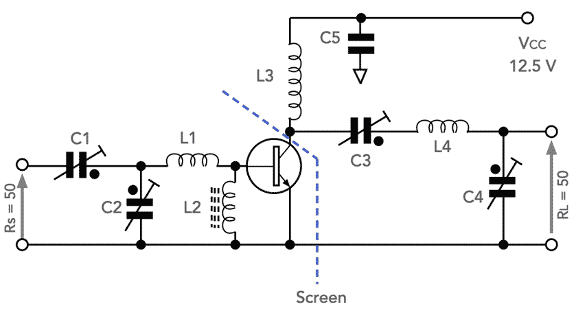
The circuit was intended as a test circuit for the 2N3553 but can be used as the basis of an RF power output or driver circuit.
The values for 175 MHz test circuit can be:
C1, C2, C3, C4 4.0 - 29pF air trimmer (dot indicates live end)
C5 10nF polyester (ceramic would be fine)
C6 100pF ceramic
L1 = 1 turn 1mm copper wire, internal diameter 10mm, leads 2 x 10mm
L2 = Ferrocube choke coil. Z at 175 MHz = 550Ω part number 4312 020 36640
L3 = 15 turns closely wound 0.7mm enamelled copper wire internal diameter 4mm
L4 = 3 turns closely wound 1.5 mm enamelled copper wire internal diameter 12 mm with leads 2 x 20mm
The maximum length for the emitter lead should be no more than 1.5mm.
 Written by Ian Poole .
Experienced electronics engineer and author.
Return to Component Data menu . . .