Home » Component data » Transistor data » this page
BLY34 Transistor Data
Transistor data for the BLY33 RF power transistor including the main electrical parameters, its pinout, package type and many other key transistor datasheet details.
The BLY34 is intended for use as an RF power output amplifier for the transmitters in small VHF radio transmitters. It is described in the datasheet as a silicon planar NPN high frequency medium power transistor intended for class B operation in VHF amplifiers.
The BLY34 has a companion BLY33 transistor which is very similar but has higher maximum voltages.
The lower voltages of the BLY34 show it is intended more for FM operation whereas the higher voltages of the BLY33 enable it to be used for AM where the envelope will mean the voltages may reach double the steady state values.
The datasheet only gives examples for the BLY34 for FM operation.
Key details and performance parameters for the BLY33 transistor.
| Transistor parameters & data |
|
|---|---|
| Parameters | Details |
| Transistor type | NPN silicon RF power transistor |
| Package type | TO39 |
| VCBO max (V) | |
| VCEO max (V) | 20 |
| VEBOmax (V) | 4.0 |
| IC max (mA) | 1500 peak |
| TJ Max °C | 150 |
| PTOT W | 2 |
| fT min (MHz) | 450 typical |
| COB | 11pF typical, 15pF max |
| hfe | |
| IC for hfe | |
| Similar / equivalents | |
Outline:
![]()
Pinout:
![]()
Note: the collector is electrically connected to the case. As a result, care needs to be taken not to short it to other connections or to ground.
Explanation of transistor parameters
| Parameter | Explanation |
|---|---|
| VCBO Max | Maximum collector-base voltage with emitter open circuit . |
| VCEO Max | Maximum collector-emitter voltage with base open circuit. |
| VEBO Max | Maximum emitter-base voltage with collector open circuit. |
| VCEsat (included where applicable) | The voltage drop across the collector-emitter when the transistor is fully saturated (acting as a closed switch). |
| IC Max | Maximum collector current. |
| Parameter | Explanation |
|---|---|
| TJ | Maximum junction temperature. |
| PTOT Max | Maximum device dissipation normally in free air at 25°C unless other conditions indicated. |
| fT Min | Minimum cutoff frequency at which the current gain in a common emitter circuit falls to unity. |
| COB Max | Maximum collector capacitane, normally measured with emitter open circuit. |
| hFE | DC current gain for HFE at IC. [Note hfe is the small signal gain and although this may be slightly different, the transistor current gain will vary considerably from ne transistor to the next of the same type.] |
| PTOT Max | Maximum device dissipation normally in free air at 25°C unless other conditions indicated. |
These are the main transistor parameters that have been included in our list. There are others, but these help quantify the main elements of the performance of the transistor.
Please note, that the data given is the best estimate we can give within a tabulated summary of this nature. Parameters also vary between manufacturers. Electronics Notes cannot accept any responsibility for errors, inaccuracies, etc, although we do endevaour to ensure the data is as accurate as possible.
Notes and supplementary information
The BLY34 was a popular RF power transistor used for a variety of RF VHF driver and output circuits. It was intended for small VHF transceivers.
• Availability & sources
The device is not widely stocked these days.
• RF performance
The data sheet for the BLY34 gives the expected performance the device as a 175 MHz common emitter amplifier providing 3.0 watts output with a typical efficiency of 80% running with a 13.5 volt supply in FM only operation.
It is recommended tat a heatsink with a thermal resistance of at least 20°K / W is recommended for operation in ambient temperatures. At air temperatures greater than 65°C it is necessary to derate the operation of the device.
It was also noted that under the recommended AM operating conditions but without any modulation, the transistor was able to withstand any load mismatch. (This was not surprising since a complete mismatch wold double the voltage seen, as would the peak voltage for amplitude modulation).
When modulation is applied, it was stated that operation into an extreme mismatch could cause damage, and adversely affect the life of the device.
• RF amplifier circuit
A basic RF amplifier circuit that could be used for the BLY34 is given below.
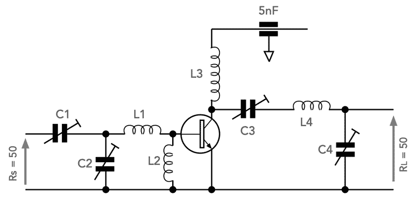
The circuit was intended as a test circuit for the BLY33 but can be used as the basis of an RF power output or driver circuit.
The values for 175MHz can be:
C1 to C4 30pF VHF types
L1 = 1 inch 18 SWG wire
L2 = 3 turns 24 SWG wire on FX115 ferrite bead
L3 = 5 turns 18 SWG wire internal diameter 9.5 mm (3/3 inch) length 9.5mm
L4 = 3 turns 18 SWG wire internal diameter 9.5 mm (3/3 inch) length 9.5mm
It was noted that for optimum performance the emitter lead length should ot exceed 1.6mm
 Written by Ian Poole .
Experienced electronics engineer and author.
Return to Component Data menu . . .