How to Design a Non-Inverting Operational Amplifier Circuit
Details of how to design an operational amplifier, op-amp non-inverting amplifier circuit with equations, design details, circuit, calculations and design tips.
Op-amp Circuits Include:
Introduction
Circuits summary
Circuit design hints & tips
Inverting amplifier
Summing amplifier
Non-inverting amplifier
Inverting vs non-inverting circuits
Variable gain amplifier
High pass active filter
Low pass active filter
Bandpass filter
Notch filter
Comparator
Schmitt trigger
Multivibrator
Bistable
Integrator
Differentiator
Wien bridge oscillator
Phase shift oscillator
 Check out my Op-Amp eBook. Check out my Op-Amp eBook. |
The non-inverting amplifier configuration is one of the most popular and widely used forms of operational amplifier circuit and it is used in many electronic circuit designs.
The op amp non-inverting amplifier circuit provides a high input impedance along with all the advantages gained from using an operational amplifier.
Although the basic non-inverting op amp circuit requires the same number electronic components as its inverting counterpart, it finds uses in applications where the high input impedance is of importance.
Video: Op-Amp Non-Inverting Amplifier Circuit
Non-inverting amplifier circuit
One of the first stages in the design is to determine that actual level of gain that is required as this is often one of the key parameters in any design.
The basic electronic circuit for the non-inverting operational amplifier is relatively straightforward.
In this electronic circuit design the signal is applied to the non-inverting input of the op-amp. In this way the signal at the output is not inverted when compared to the input.
However the feedback is taken from the output of the op-amp via a resistor to the inverting input of the operational amplifier where another resistor is taken to ground. It has to be applied to the inverting input as it is negative feedback.
It is the value of these two resistors that govern the gain of the operational amplifier circuit as they determine the level of feedback.

Non-inverting amplifier gain
The gain of the non-inverting circuit for the operational amplifier is easy to determine. The calculation hinges around the fact that the voltage at both inputs is the same. This arises from the fact that the gain of the amplifier is exceedingly high. If the output of the circuit remains within the supply rails of the amplifier, then the output voltage divided by the gain means that there is virtually no difference between the two inputs.
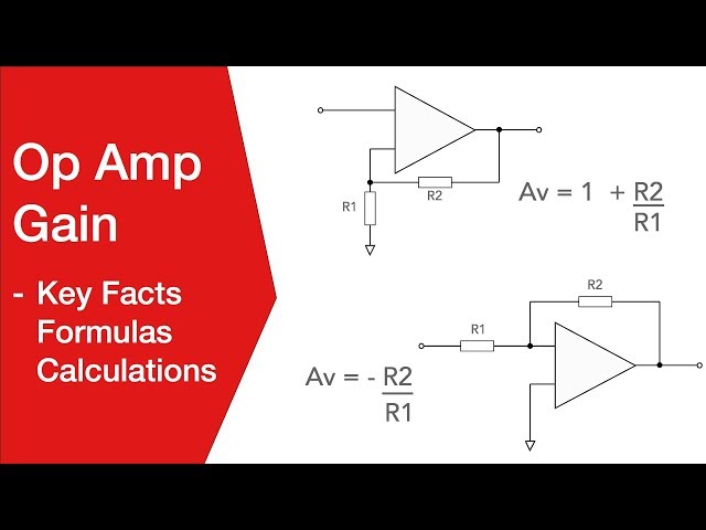
As the input to the op-amp draws no current this means that the current flowing in the resistors R1 and R2 is the same. The voltage at the inverting input is formed from a potential divider consisting of R1 and R2, and as the voltage at both inputs is the same, the voltage at the inverting input must be the same as that at the non-inverting input. This means that Vin = Vout x R1 / (R1 + R2). Hence the voltage gain of the circuit Av can be taken as:
Where:
Av = voltage gain of op amp circuit
R2 = feedback resistor resistance in Ω
R1 = resistance of resistor to ground in Ω
As an example, an amplifier requiring a gain of eleven could be built by making R2 47 k ohms and R1 4.7 k ohms.
Non-inverting amplifier input impedance
The impedance of the op amp non inverting circuit is particularly high - in fact this is often one of the key features of this circuit design.
The input impedance of this operational amplifier circuit may typically be well in excess of 107Ω.
For most circuit applications any loading effect of the circuit on previous stages can be completely ignored as it is so high, unless they are exceedingly sensitive.
This is a significant difference to the inverting configuration of an operational amplifier circuit which provided only a relatively low impedance dependent upon the value of the input resistor.
Design hints and tips
The op amp non-inverting amplifier is very easy to design, but as with any electronic circuit design there are a few points to be considered.
- Don’t make R2 too high: Although the input impedance of op amps is high, in any op amp circuit it is always best to ensure that the value of R2 is not chosen to be too high otherwise other circuit effects may load it and the value of gain may not be what is expected. It is often wise to keep the value of R2 below 100kΩ as a rough rule of thumb.
- Keep the gain down: One of the points to remember when designing with op amps, is not to expect too much gain.Even though the open loop gain can be very high, do not expect that enormous gains can be achieved over the whole of the bandwidth with minimum distortion. Think carefully when the voltage gain goes over, say, about 10 to 20.
- Remember bandwidth: Although op amps have a high value of gain, this starts to fall at increasing frequencies. Even with feedback in the inverting amplifier, the gain bandwidth product needs to be considered. Don’t try to get too much gain out of a single stage op amp circuit, otherwise the frequency response may suffer.
Ensure the output doesn't clip: For most circuits, minimising the distortion is important. One of the circuit design considerations must be to ensure that there is sufficient margin on the output so that the maximum output voltage does not approach the supply rail causing the output to clip.
Often this can happen when large amounts of gain are used, so it is worth making calculations about the maximum output voltage at an early part of the design.
AC coupling a non-inverting amplifier
In most cases it is possible to DC couple the circuit. Where AC coupling is required it is necessary to ensure that the non-inverting has a DC path to earth for the very small input current that is needed to bias the input devices within the IC.
This can be achieved by inserting a high value resistor, R3 in the diagram, to ground as shown below. The value of this may typically be 100kΩ or more. If this resistor is not inserted the output of the operational amplifier will be driven into one of the voltage rails.

When inserting a resistor in this manner it should be remembered that the capacitor-resistor combination C1 / R3 forms a high pass filter with a cut-off frequency. The cut off point occurs at a frequency where the capacitive reactance is equal to the resistance.
Similarly the output capacitor should be chosen so that it is able to pass the lowest frequencies needed for the system. In this case the output impedance of the op amp will be low and therefore the largest impedance is likely to be that of the following stage.
Single supply non-inverting amplifier
Operational amplifier circuits are normally designed to operate from dual supplies, e.g. +9V and -9V. This is not always easy to achieve and therefore it is often convenient to use a single ended or single supply version of the electronic circuit design. This can be achieved by creating what is often termed a half supply rail.
The non-inverting op amp circuit is biased at half the rail voltage. By setting the operating point at this voltage the maximum swing can be obtained on the output without clipping.

When using this circuit there are a few are a few points to note:
- Bias voltage: The bias voltage for the non-inverting amplifier is set up by R3 and R4. Normally the input impedance of the op amp itself will be higher than the resistors and therefore it can be ignored. Typically the bias voltage is set to half the rail voltage to enable the output to be able to swing equally in either direction without clipping. R3 and R4 will normally be the same value.
- Input impedance: The input impedance of this arrangement will be lower that that of the op amp on its own. The input impedance of the whole non-inverting amplifier circuit will be R3 in parallel with R4 in parallel with the input impedance of the op amp. In reality this normally equates to R3 in parallel with R4, i.e. (R3 x R4) / R3 + R4).
- Capacitor C3: The leakage of capacitor C3 must be very low otherwise the leakage current will upset the circuit and it will run into the rail. Electrolytic capacitors do not work in this position as their leakage current is too high and the circuit runs into the supply rail.
- Input & output capacitors: As with any electronic circuit design, the input and output capacitors must be chosen to pass the lowest frequencies without undue attenuation.
The non-inverting amplifier configuration using an operational amplifier is particularly useful for electronic circuit designs in electronic devices where a high input impedance is required. The non-inverting amplifier circuit is easy to build, and operates reliably and well in practice.
 Written by Ian Poole .
Experienced electronics engineer and author.
Essential operational amplifier data:-
Make your op-amp selection with op-amp data as well as distributor price and availability.
Check it out now!
More Circuits & Circuit Design:
Op Amp basics
Op Amp circuits
Power supply circuits
Transistor design
Transistor Darlington
Transistor circuits
FET circuits
Circuit symbols
Return to Circuit Design menu . . .


