Transistor Configurations: circuit configurations
Transistor circuits use one of three transistor configurations: common base, common collector (emitter follower) and common emitter - one is selected during the electronic circuit design process.
Transistor Circuit Design Tutorial Includes:
Transistor circuit design
Circuit configurations
Common emitter
Common emitter circuit design
Emitter follower
Common base
See also:
Transistor circuit types
When considering the electronic circuit design for a transistor circuit there are three different basic circuit configurations that can be used.
The three different transistor circuit configurations are: common emitter, common base and common collector (emitter follower), these three circuit configurations have different characteristics and one type will be chosen for a circuit dependent upon what is required.
Each has different properties in terms of the gain, and input and output impedance, etc and as a result, a particular configuration will be selected during the electronic circuit design process.

Each of the different transistor topologies has the inputs and outputs applied to different points, with one terminal common to both input and output.
In addition to selecting the right circuit configuration or topology in the electronic circuit design stage, to provide the required basic performance, additional electronic components are placed around the transistor: typically resistors and capacitors, and the values are calculated to give the exact performance needed.
Both the selection of the topology and the calculation of the electronic component values are key elements of the electronic circuit design process.
Transistor circuit configurations
The naming of the three basic transistor configurations indicates the transistor terminal that is common to both input and output circuits. This gives rise to the three terms: common base, common collector and common emitter.
Video: Transistor Circuit Configurations: Common emitter, common collector, common base
The term grounded, i.e. grounded base, grounded collector and grounded emitter may also be used on occasions because the common element signal is normally grounded.
There are equivalent circuit configurations for FETs, and also thermionic valves / vacuum tubes. These configurations have the same types of properties, although slightly modified for the type of electronic device used.
For FETs terms like common drain, common source and common gate are used, and for valves / tubes, terminology includes common cathode, common anode and common grid.
Common base transistor configuration
Alphabetically, this is the first transistor configuration, but it is probably the least likely to be used.

This transistor configuration provides a low input impedance while offering a high output impedance. Although the voltage is high, the current gain is low and the overall power gain is also low when compared to the other transistor configurations available. The other salient feature of this configuration is that the input and output are in phase.
This transistor configuration is probably the least used, but it does provide advantages that the base which is common to input and output is grounded and this has advantages in reducing unwanted feedback between output and input for various RF circuit design applications. This occurs because the base, which is the electrode physically between the emitter and collector is grounded, thereby providing a barrier between the two.
As a result, the common base configuration tends to be used for RF amplifiers where the increased isolation between input and output gives a greater level of stability and reduces the likelihood of unwanted oscillation. As anyone involved in RF design will attest, this is a very useful attribute.
Also the low input impedance can often able this to provide a good match to 50Ω, a useful attribute for many RF design scenarios.

Common collector (emitter follower)
The common collector circuit configuration is possibly more widely known as the emitter follower because the emitter voltage follows that of the base, although lower in voltage by an amount equal tot he turn on voltage of the base emitter junction.
The common collector, emitter follower offers a high input impedance and a low output impedance. The voltage gain is unity, although current gain is high. The input and output signals are in phase.
In view of these characteristics, the emitter follower configuration is widely used as a buffer circuit providing a high input impedance to prevent loading of the previous stage, and a low output impedance to drive following stages.

As can be seen from the diagram, in this transistor configuration, the collector electrode is common to both input and output circuits. A few additional electronic components are used with a resistor for the emitter, possibly capacitors at the input and output and bias resistors on the base if needed. In some instances, the emitter follower may be directly coupled to the previous stage as the output DC voltage may be suitable to be accommodated by the follower circuit. This means that very few additional electronic components are needed.
Common emitter transistor configuration
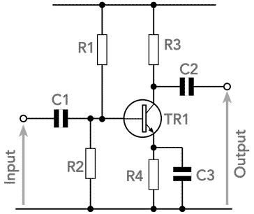
This transistor configuration is probably the most widely used. The circuit provides a medium input and output impedance levels. Both current and voltage gain can be described as medium, but the output is the inverse of the input, i.e. 180° phase change. This provides a good overall performance and as such it is often the most widely used configuration.

As can be seen from the diagram, in this transistor configuration, the emitter electrode is common to both input and output circuits.
Transistor circuit configuration summary table
The table below gives a summary of the major properties of the different transistor configurations. Not only is gain a major aspect when designing a transistor circuit, but so too are parameters like input and output impedance.
| Transistor Configuration Summary Table |
|||
|---|---|---|---|
| Transistor Configuration | Common Base | Common Collector (Emitter Follower) |
Common Emitter |
| Voltage gain | Medium | Low | Medium |
| Current gain | Low | High | Medium |
| Power gain | Low | Medium | High |
| Input / output phase relationship | 0° | 0° | 180° |
| Input resistance | Low | High | Medium |
| Output resistance | Medium | Low | Medium |
Additional electronic components
Whatever form of transistor confirmation is chosen in the electronic circuit design stage, additional components will be needed around the transistor: resistors to set the bias points and capacitors to provide the coupling and decoupling.

In this circuit of the common emitter amplifier, the basic configuration sets the basic circuit conditions of medium input impedance, medium output impedance, reasonable voltage gain and the like. The additional electronic components are then calculated to give the required operating conditions beyond this.
Each of the electronic components needs to be calculated during the electronic circuit design stage to give the required performance.
Although the common emitter will probably be seen most often with electronic components like resistors and capacitors, when used for RF circuit design, components like inductors, and transformers may also be incorporated into the circuit. The same is true for the other transistor circuit configurations as well.
Transistor circuit configurations summary infographic
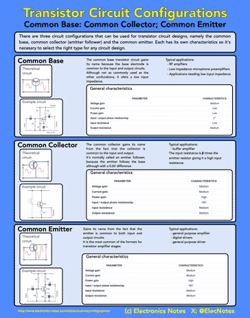
To summarise the various circuit configurations, their typical circuits and their characteristics, I've produced a summary infographic.

Click on image for larger version
The most commonly used circuit configuration is the common emitter - this is used for many amplifier stages providing voltage gain. The emitter follower or common collector is also widely used. Providing a high input impedance and low output impedance it acts as a buffer and provides only current gain - its voltage gain is unity. The common base is used in more specialist applications and is seen considerably less.
 Written by Ian Poole .
Experienced electronics engineer and author.
Essential bipolar transistor data:-
Make your BJT transistor selection with op-amp data as well as distributor price and availability.
Check it out now!
More Circuits & Circuit Design:
Op Amp basics
Op Amp circuits
Power supply circuits
Transistor design
Transistor Darlington
Transistor circuits
FET circuits
Circuit symbols
Return to Circuit Design menu . . .


