What is an FPGA - Field Programmable Gate Array: what it is,how it works
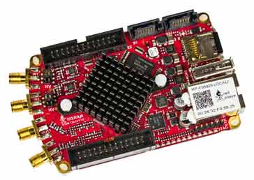
An FPGA, field-programmable gate array is an integrated circuit into which firmware is loaded which defines the functionality of the chip - this firmware can easily be changed by installing new firmware.
Home » Electronic components » this page
Programmable Logic Devices Includes:
Types of Programmable Logic Device
FPGA: Field Programmable Gate Array
The Field Programmable Gate Array, or FPGA is a programmable logic device that can have its internal configuration set by software or as it is termed, “firmware.”
This enables the FPGA functionality to be updated or even totally changed as required, because the FPGA firmware is updated when it is in circuit.

The FPGA programmable logic components, or logic blocks as they are known, may consist of anything from logic gates, through to memory elements or blocks of memories, or almost any element.
This provides a considerable degree of flexibility.
FPGA applications
The reconfigurable nature of the FPGA means that it can be used in a wide number of different applications.
FPGAs are used in a host of different areas where complex logic circuits and systems are needed - from various logic circuits to high performance processors.
- ASIC prototyping: ASICs or application specific integrated circuits are often used in high volume production, but they are very costly to develop and changes are very expensive and time consuming to make. Once an ASIC chip is made, its functionality is fixed. Also ASIC chips are typically very complicated and to ensure that the functionality is correct, often an FPGA is used instead of the ASIC chip during development and even early production until all the issues are removed.
- Software defined equipment: With equipment now tending more towards being software defined as in the case of the software defined radio the concept is being widely used in many areas of technology. Software defined test equipment is also becoming more widely used - here the functionality of the test instrument can be modified according to what is needed.
- Digital Signal Processing (DSP): The ability to implement complex algorithms efficiently makes FPGAs ideal for applications like signal filtering, modulation, and data compression. Their speed copared to other forms of logic makes them ideal for this. They are also reconfigurable, making them ideal for use in software defined radios which can be reconfigured to meet changing requirements.
- High-Performance Computing (HPC): FPGAs can be used as accelerators within HPC systems to offload specific tasks, improving overall performance.
- Embedded Systems: Due to their small size and low power consumption options, FPGAs can be integrated into embedded systems for custom logic and real-time processing needs.
- Medical Imaging: Reconfigurable logic within FPGAs enables real-time image processing and data analysis in medical imaging applications.
- Networking: FPGAs can be employed in network equipment for tasks like packet processing and traffic management.
FPGA vs ASIC
FPGAs and ASICs can often be seen to have comparatively similar functions, i.e. that of providing a large amount of specific logic functionality within a circuit.
However there are significant differences between ASICs and FPGs and this means that they are used in different areas.
Although FPGAs offer many advantages, there are naturally some disadvantages. They are slower than equivalent ASICs (Application Specific Integrated Circuit) or other equivalent ICs, and additionally they are more expensive. (However ASICs are very expensive to develop by comparison).
This means that the choice of whether to use an FPGA based design should be made early in the design cycle and will depend on such items as whether the chip will need to be re-programmed, whether equivalent functionality can be obtained elsewhere, and of course the allowable cost. Sometimes manufacturers may opt for an FPGA design for early product when bugs may still be found, and then use an ASIC when the design is fully stable.
FPGAs are used in many applications. In view of the cost they are not used in cheap high volume products, but instead FPGAs find applications in a variety of areas where complex logic circuitry may be needed, and changes may be anticipated. FPGA applications cover a wide range of areas from equipment for video and imaging, to circuitry for aerospace and military applications, as well as electronics for specialized processing and much more.
Here is a summary of the differences:
| Comparison of FPGA v ASIC |
||
|---|---|---|
| Attribute | FPGA | ASIC |
| Development Cost | Medium | High |
| Development timescale | Low to medium | Long |
| Unit cost in large production | High | Low |
| Reconfigurability | Easy | Not possible |
| Speed of operation | Slower than ASIC | Very fast |
| Power consumption | Tends to be higher | Normally lower |
| Manufacture | Off the shelf purchase and in-house or in-equipment programming | Lengthy manufacturing cycle |
| Area efficiency | Lower | Higher |
As a result of the characteristics of FPGAs and ASICs, FPGAs tend to be used for development and lower volume production, whereas ASICs tend to be used for higher performance, overall lower cost in large quantities and faster performance.
FPGA basics
The great advantage of the FPGA is that the chip is completely programmable and can be re-programmed. In this way it becomes a large logic circuit that can be configured according to a design, but if changes are required it can be re-programmed with an update.
Thus if circuit card or board is manufactured and contains an FPGA as part of the circuit, this is programmed during the manufacturing process, but can later be re-programmed to reflect any changes.
FPGA internals
The internal architecture of the FPGA is the key to its flexibility and hence its success. Essentially an FPGA consists of two basic elements:
Common logic blocks, CLBs: These are the fundamental units of logic within an FPGA. They contain an array of logic gates (AND, OR, NOT, etc.) and flip-flops (memory elements) that can be interconnected in various configurations.
The logic block in an FPGA can be implemented in variety of ways. The actual implementation depends upon the manufacturer and also the series of FPGA being used. The variations include the number of inputs and outputs, the general complexity of the logic block in terms of circuitry and the number of transistors used. This naturally has an impact on the amount of area consumed on the chip, and hence the size the silicon used.
FPGA internal routing & programmable interconnections: The routing channels within the FPGA comprise wires that can be interconnected using electrically configurable switches. In this way it is possible to link different points on the chip together and thereby connect the different Common Logic Blocks in whatever way is required.
Input/Output (I/O) Blocks: These interfaces connect the FPGA to the external world, allowing it to receive data and send processed information.
FPGA firmware development
As the FPGA is a configurable logic array, the logic needs to be set to meet the requirements of the system. The configuration is provided by firmware - a set of data that is
In view of the complexity of FPGAs, software is used to design the function of an FPGA. The FPGA design process is started by the user providing a Hardware Description Language (HDL) definition or a schematic design.
Common HDLs are VHDL (where VHDL stands for VHSIC Hardware Description Language) and Verilog.
Once this has been completed the next task in the FPGA design process is to produce a netlist is generated for the particular FPGA family being used. This describes the connectivity required within the FPGA and it is generated using an electronics design automation tool.
The netlist can then be fitted to the actual FPGA architecture using a process called place-and-route, usually performed by the FPGA company's proprietary place-and-route software.
Finally the design is committed to the FPGA and it can be used in the electronic circuit board for which it is intended.
Note on the FPGA programming:
FPGAs require firmwave to be available to set the configuration of the logic within the chip. This firmwave can be developed in a variety of ways and there are several different software platforms that can be used.
Read more about the FPGA programming
FPGA testing
In view of their complexity, it is necessary to undertake rigorous testing of the FPGA design. This testing will normally be undertaken at each stage of the FPGA development process.
It includes functional simulation, and other verification methodologies, but one of the key issues can be that of timing as the size and complexity of the basic logic can mean that timing issues can arise.
Once the design and validation process is complete, the binary file generated (also using the FPGA company's proprietary software) is used to configure the FPGA device.
FPGA tools
The tools for developing and testing FPGAs are available from a variety of sources. Obviously the manufacturer is able to offer many FPGA development tools, but there are many other sources for third party FPGA HDL synthesis, FPGA physical synthesis and verification tools. These include the actual development and for the various stages of testing of the FPGAs.
 Written by Ian Poole .
Experienced electronics engineer and author.
More Electronic Components:
Batteries
Capacitors
Connectors
ADC
DAC
Diodes
FET
Inductors
Memory types
Phototransistor
Quartz crystals
Relays
Resistors
RF connectors
Switches
Surface mount technology
Thyristor
Transformers
Transistor
Unijunction
Valves / Tubes
Return to Components menu . . .


