RS Flip Flop Circuit
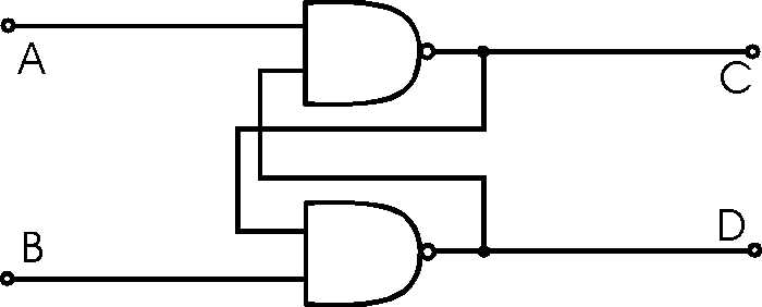
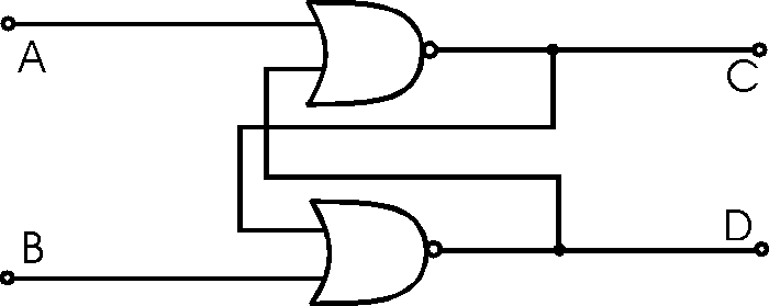
- two logic or digital circuits for an RS flip flop, one using NAND gates and the other RS flip-flop using NOR gates.
Logic / Digital Design Includes:
Logic gate types
Logic truth table
How to convert NAND / NOR gates with inverters
Exclusive OR, XOR
RS Flip-Flop
Edge triggered RS Flip-Flop
Programmable inverter
D-type frequency divider
RS flip flops find uses in many applications in logic or digital electronic circuitry. They provide a simple switching function whereby a pulse on one input line of the flip flop sets the circuit in one state. Further pulses on this line have no effect until the R-S flip flop is reset. This is accomplished by a pulse on the other input line. In this way the R S flip flop is toggled between two states by pulses on different lines.
Although chips are available with R-S functions in them, it is often easier to create an R-S flip flop from spare gates that may already be available on the board, or on a breadboard circuit using a chip that may be to hand. To make an R S flip flop, it simple requires either two NAND gates or two NOR gates.
Using two NAND gates and active low R S flip flop is produced. In other words low going pulses active the flip flop. As it can be seen from the circuit below, the two incoming lines are applied, one to each gate. The other inputs to each of the NAND gates are taken from the output of the other NAND gate.
It can be seen from the waveform diagram that a low going pulse on input A of the flip flop forces the outputs to change, C, going high and D going low. A low going pulse on input B then changes the state, with C going low and D going high.

The circuit for the NOR version of the circuit is exceedingly similar and performs the same basic function. However using the NOR logic gate version of the R S flip flop, the circuit is an active high variant. In other words the input signals need to go high to produce a change on the output. This may determine the choice of integrated circuit that is used. Although the NAND gate version is probably more widely used, there are many instances where the NOR gate circuit is of value.

These circuits are widely used in many electronic logic circuit applications. There are also contained within many integrated circuits where they are a basic building block. As such the R S flip flop is an exceedingly popular circuit.
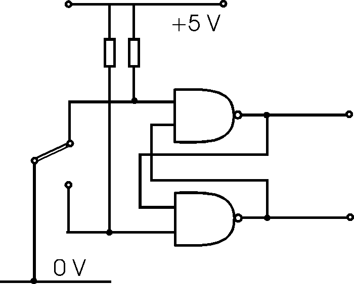
One useful application for a simple R S flip flop is as a switch de-bounce circuit. When any mechanical switch makes or breaks contact, the connection will make and break several times before the full connection is made or broken. While for many applications this may not be a problem, it is when the switch interfaces to logic circuitry. Here a series of pulses will pass into the circuit, each one being captured and forming a pulse. Dependent upon the circuit this may appear as a series of pulses, and falsely triggering circuits ahead of time.

It is possible to overcome this problem using a simple RS flip flop. By connecting the switch as shown below, the flip flop will change on the first sign of contact being made. Further pulses will not alter the output of the circuit. Only when the switch is turned over to the other position will the circuit revert to the other state. In this way a simple two gate circuit can save the problems of de-bouncing the switch in other ways.
 Written by Ian Poole .
Experienced electronics engineer and author.
More Digital Logic and Embedded Topics:
FPGA programming
Embedded systems
How a computer works
Logic circuit design basics
Logic / circuit design guidelines
Return to Digital / Logic / Processing menu . . .


