Boundary Scan, JTAG, IEEE 1149 Tutorial
A summary, overview or tutorial of the basics of what is boundary scan, JTAG, IEEE 1149 (IEEE 1149.1), test system used for testing complex electronic circuits where there is limited test access.
Boundary Scan JTAG Includes:
What is Boundary Scan / JTAG
Boundary scan description language, BSDL
Design for test with boundary scan
JTAG Spec & IEEE 1149 Standard
JTAG TAP & connector
IEEE 1149.6 (AC coupled JTAG)
Compact JTAG cJTAG IEEE 1149.7
IJTAG, IEEE 1687
Since its introduction in the early 1990s, boundary scan, also known as JTAG or IEEE 1149, has become an essential tool used for testing boards in development, production and in the field. JTAG, boundary scan is a test technique that enables information about the state of a board to be gained when it is not possible to gain access to all the nodes that would be required if other means of test were used.
In view of the way in which the density of boards has been increasing in recent years, it is normally very difficult to be able to probe electronic circuits and gain the information that is required to test these boards. As JTAG, boundary scan enables much of a board to be tested with only minimal access, it is now widely used for the test of electronic circuits at all stages of their life. In view of the fact that other forms of test require access either in terms of bed of nails fixtures, while others need to probe a variety of places on the board, boundary scan offers a unique solution to many test requirements.
Although the JTAG, boundary scan technique is aimed at testing circuits, its flexibility enables it to be used for a wide variety of applications including test applications:
- System level test
- BIST access
- Memory testing
- Flash programming
- FPGA / CPLD programming
- CPU emulation
While testing remains the major application for boundary scan, it can be see that it is also useful in other applications as well. In view of its flexibility, the technique is widely used, and a powerful tool in both development and production applications.
Boundary scan history
With the problem of lack of test access to boards starting to become a problem, a group known as the Joint Test Action Group (JTAG) was set up in 1985. Its aim was to address the issues being faced by electronics manufacturers in test strategies and to enable tests to be undertaken where no other technologies could gain access.
The introduction of surface mount technology and further miniaturisation had meant that people feared access to boards for testing would be severely limited. To overcome this, new strategies would be required.
The original goal for boundary scan was to complement existing techniques including in-circuit test, functional built in test and other techniques and to provide a standard that would enable the testing digital, analogue and mixed signal circuits.
The standard for boundary scan that was devised has been adopted by the Institute or Electrical and Electronics Engineers, IEEE in the USA as IEEE 1149. The first issue of the standard, IEEE 1149, was in 1990. The stated purpose of IEEE 1149 was to test the interconnections between integrated circuits mounted on boards, modules, hybrids and other substrates. As most of the problems occurring with electronics circuits occur with the interconnections, the IEEE 1149 test strategy would reveal most of the problems.
In 1993, a revised version of the boundary scan, IEEE 1149 standard was issued which contained many clarifications, enhancements and corrections. Then in 1994, a further issue of the IEEE 1149 standard took place. This introduced the Boundary Scan Description Language, BSDL. This enabled boundary scan tests to be written in a common language, thereby improving the way in which tests could be written and code re-used, thereby saving development time.
Difference between boundary scan, JTAG and IEEE 1149.1
- Boundary scan: This refers to the test technology where additional cells are placed in the leads from the silicon to the external pins so that the functionality of the chip and also the board can be ascertained.
- JTAG: The term JTAG refers to the interface or test access port used for communication. It includes the TCK, TDI, TDO, TMS, etc, connections. For some applications this interface may be used to interrogate or communicate with internal instruments within the core of the chip.
- IEEE 1149.1: This is the IEEE standard defining test logic that can be included in an integrated circuit to provide standardized approaches for testing the interconnections to the circuit board, the integrated circuit itself, or form modifying or observing the circuit activity during normal operation of the circuit.
Boundary scan basics
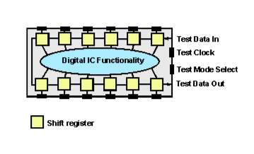
The JTAG, boundary scan test technique uses a shift register latch cell built into each external connection of every boundary scan compatible device. One boundary scan cell is included in the integrated circuit line adjacent to each I/O pin, and when used in the shift register mode it can transfer data along to the next cell in the device. There are defined entry and exit points for the data to enter and exit the device, and it is therefore possible to chain several devices together.

Under normal operating conditions the cell is set so that it has no effect and it becomes invisible. However when the device is set to test mode, it permits a serial data stream (test vector) to be passed from one shift register latch cell to the next. Boundary-scan cells in a device can capture data from integrated circuit line, or force data onto them. In this way a test system that can input a data stream to the shift register chain can set up states on the board, and also monitor data. By setting up one serial data stream, latching this into place, and then monitor the returning data stream, it is possible to gain access to the circuits on the board and check that a returning data stream is what is expected. If it is, then the test can pass, but if not the boundary scan system has detected and problem that can be further investigated.
JTAG Interface
There are a number of JTAG control and data lines that form the test access port, TAP. These lines known as TCK, TMS and the optional TRST line are connected in parallel to the chips in the boundary scan chain. Connections designated TDI (input) and TDO (output) are daisy chained together to provide a path around the boundary scan chips for the data. Data is sent into the TDI of the first chip, and then TDO from the first chip is connected to TDI of the next and so forth. Finally the data is taken from the TDO of the last IC in the daisy chain.
- TAP Test Access Port - The pins associated with the test access controller.
- TCK Test Clock - this pin is the clock signal used for ensuring the timing of the boundary scan system. The TDI shifts values into the appropriate register on the rising edge of TCK. The selected register contents shift out onto TDO on the falling edge of TCK.
- TDI Test Data Input - Test instructions shift into the device through this pin.
- TDO Test Data Output - This pin provides data from the boundary scan registers, i.e. test data shifts out on this pin.
- TMS Test Mode Select - This input which also clocks through on the rising edge of TCK determines the state of the TAP controller.
- TRST Test Reset - This is an optional active low test reset pin. It permits asynchronous TAP controller initialization without affecting other device or system logic.
Read more about the JTAG interface / TAP
Applications for boundary scan
JTAG, boundary scan is an ideal test tool for use in many applications. The most obvious applications for boundary scan are within the production environment. Here the boards can be tested and problems that might otherwise go un-detected because of lack of test access can be adequately tested. In fact boundary scan technology is being combined with other technologies to provide what is termed a combinational tester.
In addition to being used in production test, boundary scan, JTAG, IEEE 1149, can also be used in a variety of other test scenarios, including product development and debugging as well as field service. This means that the boundary scan code can be re-used for test areas, and hence the cost can be split over these applications. Not only does this indicate that boundary scan is a powerful tool, but it also makes it financially attractive.
Programme generation
One of the chief costs for any development these days is the cost of the software, and this is particularly true for boundary scan where there is little hardware. This means that any savings that can be made in the time taken for the software development can significantly reduce the costs. Accordingly a Test Programme Generator (TPG) is an integral part of a boundary scan system.
Typically the test programme generator requires the net-list of the Unit Under Test (UUT) and the Boundary Scan Description Language (BSDL) files of the boundary scan components contained within the circuit. With this information it is possible for the test programme generator to create the test patterns used for the test. These allow the system to detect and isolate any faults for all boundary-scan testable nets within the circuit. It is also possible for the test programme generator to create test vectors that enable the system to detect faults on the nodes or pins components non-boundary scan components that are surrounded by boundary scan devices
JTAG, boundary scan, IEEE 1149 is a test technique that is now well established. Although it requires test programmes to be generated before it can be used, it nevertheless provides a very cost effective method of gaining access for test vectors into an electronic circuit board. With circuit board real estate being at a premium, the cost of adding probe or access points for other type of electronic test technologies would be prohibitive, if indeed it were possible. Accordingly boundary scan provides a solution to many test problems at a cost that can be amortised over several test arenas from development through production test to field test. In all of these environments, boundary scan provides an effective solution, both in terms of performance and cost.
 Written by Ian Poole .
Experienced electronics engineer and author.
More Test Topics:
Data network analyzer
Digital Multimeter
Frequency counter
Oscilloscope
Signal generators
Spectrum analyzer
LCR meter
Dip meter, GDO
Logic analyzer
RF power meter
RF signal generator
Logic probe
PAT testing & testers
Time domain reflectometer
Vector network analyzer
PXI
GPIB
Boundary scan / JTAG
Data acquisition
Return to Test menu . . .


